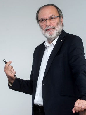
Béla Pécz, Director of the Institute of Technical Physics and Materials Science of the HAS Centre for Energy Research
The Strengthening research infrastructure – internationalisation, networking (VEKOP 2.3.3) call mirrors the similar GINOP call to make funding available for the Central Hungary region and aims to enhance the international competitiveness of the domestic research infrastructure and create competitive knowledge hubs. This contributes to the building and reinforcing successful international cooperation relations. The world-class scientific research equipment (formerly available only in foreign scientific institutes) enables Hungarian researchers to achieve internationally outstanding results at home. For a scientific hub to be attractive for foreign scientists it has to offer internationally a competitive range of equipment.
‘A 200 kV transmission electron microscope has been deployed. As a novelty, the equipment is furnished with an image corrector to handle the so-called spherical aberration,’ says Béla Pécz, Director of the Institute of Technical Physics and Materials Science of the HAS Centre for Energy Research. ‘These microscopes have only been available since 2005, and as a special ability, they can focus rays far from the optical axis in one focal point which dramatically increases resolution. The factory-guaranteed resolution of the microscope is 0.9 Angstrom, i.e. 90 picometres (0.00000000009 metres). However, on-site tests showed that actual resolution can reach up to 70 picometres.’
To better understand the extraordinary features of the microscope and the above description, it is worth taking a brief look at how transmission electron microscopes work. Electron microscopes use an electron beam instead of visible light to illuminate the sample to be magnified. In the case of transmission microscopes, the electron beam is transmitted through an ultrathin (only a few atoms thick) sample to form an image.
At the time, the need to replace visible light with another type of radiation in microscopy emerged because the wavelength of the illuminating radiation fundamentally determines the resolution of the microscope (i.e. the smallest distance that is perceived as two different points in the microscopic image). The wavelength of the electron beam is much shorter than that of visible light, resulting in higher resolution images. The resolving power of electron microscopes is more than a thousand times greater than that of light microscopes.
The electron beam is focused with lenses but a problem occurs here. If the beam does not pass exactly through the centre of the lens but closer to its edge (i.e. the axis of the beam does not coincide with the optical axis), the lens will not be able to focus the electrons exactly in the focal point, reducing the sharpness and resolution of the image. This is called spherical aberration and needs to be corrected. So, the new microscope extremely effectively corrects this aberration, resulting in exceptionally good resolution.
‘With this microscope we will be able to examine virtually any samples at atomic scale. In silicon, for instance, the network solid becomes visible at 3 Angström resolution. Hungary has never had such a microscope, so this will be the first time for us to routinely examine any matter with resolution under one Angstrom,’ the direction of the institute says. ‘Besides, the microscope can also scan the sample and map the elementary composition of the matter with highly sensitive x-ray probes. We can make the distribution of the different atoms visible as a map, even in colour.’
The researchers plan to use the microscope for examining two-dimensional materials (like graphene). They will also examine the electrical properties of semiconductors comprising only two atomic layers, or bioactive ceramic coatings covering human joint implants. Or they will be able to make silicon nitride ceramics electrically conductive by adding graphene or carbon nanotubes. The equipment will also play a key role in university education and corporate R&D projects.
 |
 |
|
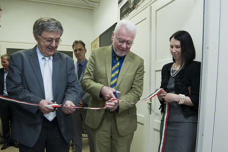
László Lovász, President of HAS and József Pálinkás, President of NRDIO cut ribbon at the ceremony |
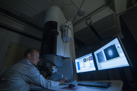
New transmission electron microscope in operation (photo: HAS / Tamás Szigeti) |
The list of further funded projects is available here.
Relating news:
Veszprém-based development to open up new perspectives on the world of particles (another research infrastructure investment financed under the GINOP-2.3.3 call)


